
Engineering
February 22, 2023
Researchers create a new etching method to improve smartphone circuit performance
In circuitry, etching is used to remove the deformed layer created during the grinding and polishing of metal components by selective chemical attack. Now, a research group at Nagoya University in Japan has developed a new method called “wet-like plasma etching” that combines the selectivity of wet etching with the controllability of dry etching. This technique will make it possible to etch new and hard-to-etch materials, enabling higher performance and lower power consumption of the silicon semiconductor integrated circuits used in smartphones and data centers. The researchers’ findings were published in the journal Scientific Reports.
In the race to create the fastest and most energy-efficient circuits for computing devices, scientists are constantly looking for new transistor designs. Recently, there has been a shift from FinFET-type transistors, so-called because the gate is raised above the silicon plane like a shark’s fin, to gate-all-around transistors, in which the fin is replaced by a stack of horizontal sheets that look like a pagoda in a Buddhist temple. In this type, the sheets surround the channel to reduce leakage and increase the drive current.
To fabricate these complex structures, metal carbides consisting of titanium (Ti) and aluminum (Al), such as TiC or TiAlC, are used as metal gates where the voltage is applied. TiAlC is a ternary material with high hardness, high wear resistance, high melting point, and excellent electrochemical performance.
There are two ways to etch such materials. Wet etching uses chemical solutions, while dry etching uses gases. Conventionally, TiAlC films used in semiconductor devices are etched by wet etching using hydrogen peroxide liquid mixtures. However, this process requires a long etching time to completely remove the target metals. It also runs the risk of chemically damaging the metal gate. Additionally, the liquids used can create surface tension at the atomic level, destroying important features.
In order to develop an advanced etching process for the selective removal of TiAlC over other Ti compounds, non-halogen etching has been tested as a possible solution. Currently, there is no non-halogen dry etching process for metal carbides made of the three elements.
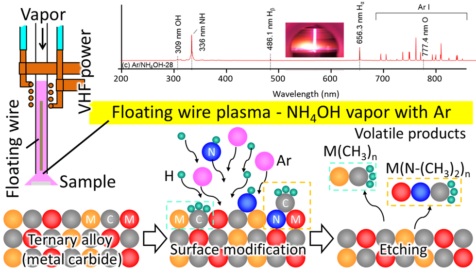
Now, a research group led by Professors Masaru Hori, Kenji Ishikawa, and Thi-Thuy-Nga Nguyen at the Center for Low-Temperature Plasma Science at Nagoya University, in collaboration with the companies Hitachi, Ltd. and Hitachi High-Tech Corp., has developed a new dry etching method for metal carbides. This method uses a floating wire-assisted vapor plasma of argon gas mixed with vapor sources of ammonium hydroxide-based mixtures at medium pressure. In the circuit, the plasma is generated by adding energy to the gas, so the additional floating wire can enhance the generation of high-density plasma. Since this process generates active radicals of H, NH, and OH from the ammonium hydroxide gas (NH4OH), the treated surface of TiAlC can be removed after surface modifications of the TiAlC film.
“Atmospheric pressure plasma and medium-pressure plasma techniques are used to miniaturize equipment size, fabrication cost, and energy consumption,” explained Ishikawa. “It is difficult to etch off compounds involving multiple elements. Therefore, control of surface modification plays a key role. Our group investigated the use of various radicals for surface modification and developed a method for generating such radicals using floating wire plasma and a vapor supplement. This provides a rich radical source of NH, H, and OH, which react with the TiAlC surface to form volatile products and etch the TiAlC surface.
“This floating wire-assisted plasma technique is expected to be available for highly selective etching of metals and metal compounds used in semiconductor device fabrication,” Ishikawa continued. “Metal carbides are promising gate electrode materials for advanced silicon semiconductors, and our joint research group was the first in the world to succeed in chemical dry etching of non-silicon semiconductor materials. This achievement is important for the development of atomic layer-level etching technology, which has been difficult to achieve so far. Our results represent an important milestone, and a dramatic technological leap forward, in microfabrication technology.”

Research developed a new method called “wet-like plasma etching” that combines the key features of
two existing techniques: wet etching and dry etching. (Credit: Nagoya University)
The study, "Dry etching of ternary metal carbide TiAlC via surface modification using floating wire‑assisted vapor plasma," has been published in the journal Scientific Reports at DOI: 10.1038/s41598-022-24949-1
Authors:
Thi-Thuy-Nga Nguyen, Kazunori Shinoda, Hirotaka Hamamura, Kenji Maeda, Kenetsu Yokogawa, Masaru Izawa, Kenji Ishikawa, and Masaru Hori
Media Contact:
Matthew Coslett
International Communications Office, Nagoya University
kouho-en@adm.nagoya-u.ac.jp

